Flip-Flops
- Usha Saha

- Sep 23, 2020
- 5 min read
Updated: Sep 25, 2024
Flip-Flops comes under the category of sequential circuits, the question here would be why to study sequential circuits? The purpose is very clear as many digital systems generate outputs depending on past values, so for this, a system must have memory for the storage of data but combinational circuits are memoryless circuits. Therefore the usages of sequential circuits come into practice as these are circuits with memory.
In this article we would study flip-flops from the competitive exam viewpoints, incorporating the entire Flip-Flop topics form block Diagram to excitation table. Such that all the essential concept necessary for the exam is present beneath one roof.
Sequential Circuits
A sequential circuit at any instant of time depends not only on the present values of inputs but also depends on the past values; this is the major difference between a combinational circuit and a sequential circuit. This dependency of the system on the past history makes a sequential circuit slower, and complex in design as compared to the combinational circuits.
For more information on the combinational circuit refer to the combinational circuit article on the site.

Important terms to remember
Before heading towards the flip-flops let's have a basic knowledge about some important terms like what are synchronous and asynchronous sequential circuits, the difference between edge trigger and level trigger, and most important the difference between latches and flip-flops. Knowledge about all these terms is the prime requirement to understand flip-flops in the best way.
To start with, synchronous and asynchronous sequential circuits are the two types of sequential circuits. In the synchronous sequential circuits, the change in the input signal would affect the memory element on the activation of the clock signal. That is the memory elements are clocked flip-flops. The synchronous sequential circuits are generally edged trigger circuits.
On the other hand in the asynchronous sequential circuits the input, many affect the memory element at any instant of time. The memory elements in the asynchronous sequential circuits are unclocked flip-flops. Asynchronous sequential circuits are level triggered circuits.
Triggering
Triggering is used to initiate the operation of the latches or the flip-flops. Triggering are of two types;
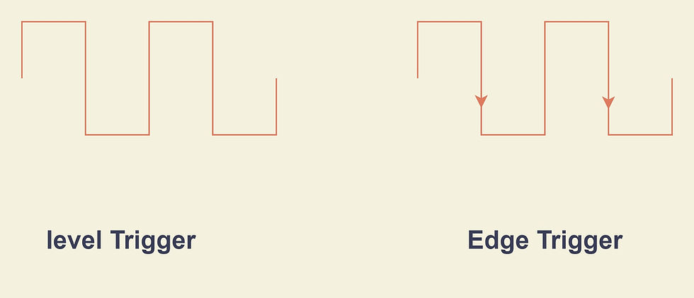
Level Trigger
In level triggering the input affects the flip-flops when the clock is at logic 1, this implies that in level triggering the output can change several times in a single clock pulse.
Edge Trigger
In edge triggering the input signal affects the flip-flops only if they are present at the negative or positive-going edge of the clock pulse that is in edge triggering the output would only change once in a single clock pulse.
Latches and Flip-flops
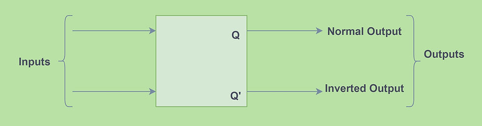
A flip-flop is made up of logic gates in such ways that altogether the logic gates permit storage capacity to the flip-flop. Due to this, a flip-flop is called a one-bit memory element. A flip-flop has two stable states therefore also called a bistable multivibrator. A flip-flop in its simplest form is called a latch. A latch is basically level triggered, whereas a flip-flop is an edge trigger.
Types of Flip-Flops
S-R flip-flop
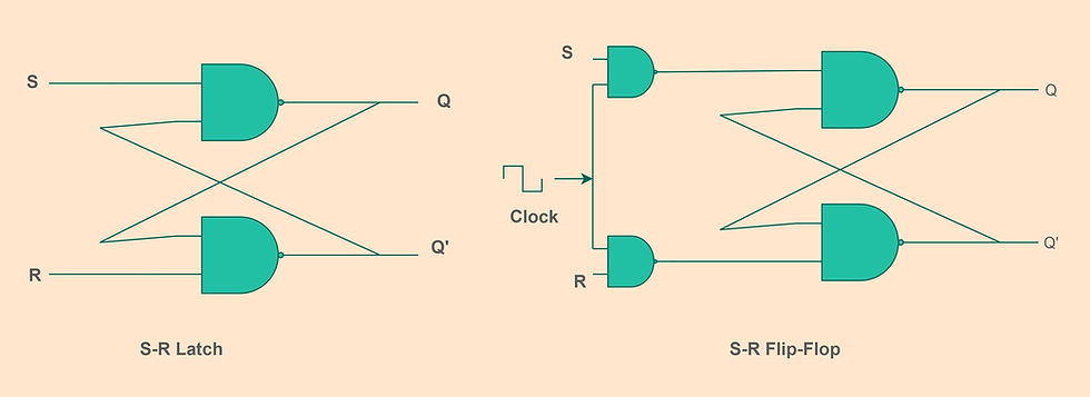
An S-R flip-flop is similar to an S-R latch with a clock signal additional in it. The input elements are S and R, and the output elements are Q and Q'. Let us understand the S-R flip-flop in a better way with the truth table, characteristics equation, and excitation table. The image below shows the S-R latch and S-R flip-flop representation using NAND gates, the same can be done with the NOR gate. The only difference using the NOR gate is, that the two extra NAND gate where the clock is applied is changed with AND gate.
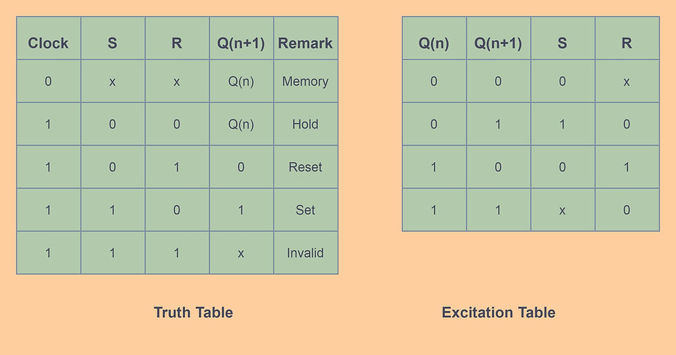
The table below shows the truth table and the excitation table. When the clock is zero the output retains the previous value. When the clock sets to one then the output change according to the input. For S=R=0 the flip-flop is at hold state. For S=0 and R=1 the flip-flop is Reset. For S=1 and R=0 the flip-flop is Set. For S=R=1 the flip-flop output is invalid.
Characteristic Equation
Q(n+1)= S+R'Q(n)
The characteristics equation is very important, as it is used in the conversion of one flip-flop to another.
The only disadvantage of S-R flip-flop is the presence of an invalid state when S=R=1. To avoid this another flip-flop is used that is J-K flip-flop.
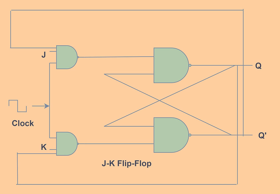
J-K Flip-Flop
A J-K flip-flop is the modified version of an S-R flip-flop. The invalid output states of the S-R flip-flop is defined in the J-K flip-flop. The inputs elements are J and K and the output elements are Q and Q'. The input lines J and K are connected to the Q' and Q respectively.
In the J-K flip-flop, the output varies in the same manner as that of S-R flip-flop, except for the J=K=1 condition. At J=K=1 the output toggles between 1 and 0.
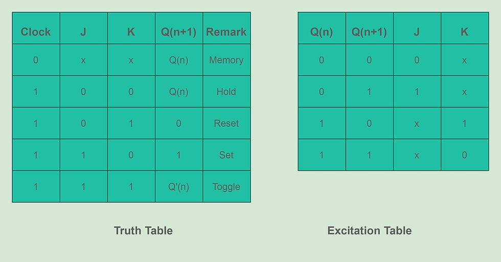
The truth-table and the excitation table are as shown.
Characteristic Equation.
The characteristic equation of a J-K flip-flop is Q(n+1)=JQ'(n)+K'Q(n)
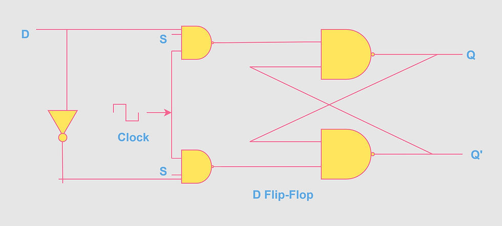
D Flip-Flop
D flip-flop is another modified version of the S-R flip-flop, which is designed in such a way that the invalid state is eliminated. The logic diagram of a D flip-flop is as shown.
The truth table and excitation table of a D flip-flop is as follows;
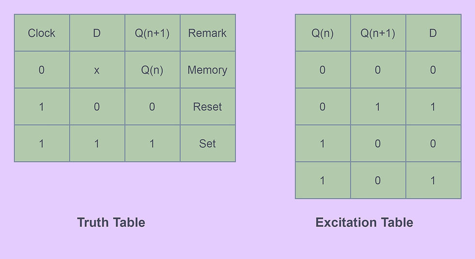
The characteristic equation of a D flip-flop is Q(n+1)=D
T Flip-Flop
The T flip-flop is a single input version of J-K flip-flop and can be designed form J-K flip-flop.
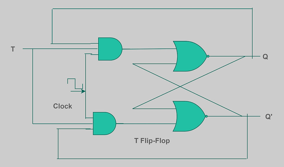
The truth table and excitation table of a T flip-flop is as follows;
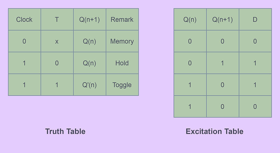
The characteristic equation of a T flip-flop is Q(n+1)= T'Q(n)+TQ'(n)
With the discussion on the T, flip-flop completes the family of flip-flops. So far the invalid condition in the S-R flip-flop is handled by the J-K flip-flop, but still, the difficultly is not completely eliminated. As the J-K flip-flop toggles at J=K=1. This is called Race Round Condition and is completely resolved by the #Master-Slave flip-flop.
A master-slave flip-flop constitutes two flip-flops one is called MASTER and the other is SLAVE.
Application of Flip-Flops
There is numerous application of flip-flops in the digital context. Some of them are
Serial to parallel converter.
Counters
Serial and parallel data storage.
Latch
As a frequency divider.
Order Electronics Projects
Want us to guide you through your project or make the project for you? Click on the button below or reach out to us via Call/WhatsApp at (+91) - 7600948607
You can -
Order Basic Electronics Projects
Order Embedded Systems Projects
Order IoT Projects
Order FPGA Projects
Order VLSI Projects
Order Image Processing Projects
Order Matlab Projects
Order TinkerCAD Projects
Order Proteus Projects
Click on the button below to fill out the project inquiry form -
Create Various Projects
Check out our Free Arduino Projects Playlist - Arduino Projects
Check out our Free Raspberry Pi Projects Playlist - Raspberry Pi Projects
Check out our Free TinkerCAD Projects Playlist - TinkerCAD Projects
Check out our Free IoT Projects Playlist - IoT Projects
Check out our Free Home Automation Projects Playlist - Home Automation Projects
Check out our Free NodeMCu Projects Playlist - NodeMCu Projects
Follow us -
Please do follow us i.e. #learnelectronicsindia to get daily updates about new blogs, videos, courses, products, offers, competitions, quizzes, and Internship Opportunities.
Bravo, Learn Electronics India! Your article on Flip-Flops was not only educational but also highly engaging. I found myself absorbed in the topic from start to finish. The inclusion of practical tips and troubleshooting advice was a thoughtful touch. It's evident that the author's expertise and enthusiasm shine through the words. Thank you for sharing such valuable knowledge.
Brilliant explanation! Thanks, LearnElectronics India!