


Transistors: Working Principle, Types, and its Applications
- NIVVETHA CHELLAPPAN
- Jan 16, 2024
- 7 min read

Updated: Sep 15, 2024
What is a transistor?
A transistor is a three-terminal semiconductor device that regulates or controls the current flow, or voltage flow, in an electronic circuit. It is one of the basic elements used in modern-day electronics. It controls the flow of the electronic signals in a circuit. A transistor is used as an amplifier or switch.

The transistor basically contains three terminals, namely,
Base (B)
Collector (C)
Emitter (E)
These three terminals of a transistor are necessary to establish a connection to an external circuit and carry current. Most transistors are made of silicon (Si) and can be made from germanium (Ge) and gallium arsenide (GaAs).
Working principle of a transistor
The current flow through one channel is controlled by varying the smaller current that is flowing through another channel.
A transistor is used to amplify and generate electrical signals.
Transistor as amplifier
It converts a small input current into a larger output current.
Transistor as Switch
It contains two different states (ON and OFF) and controls the electronic signal flow through an electrical circuit and electronic device.
Parts of the Transistor
Base (B)
Emitter(E)
Collector(C)
Base (B)
This terminal is responsible for activating the transistor.
It is present between the emitter (E) and collector (C).
This terminal is thin and highly doped.
The base passes the majority of carriers from emitter to collector.
Emitter (E)
This is the negative terminal of the transistor, and it emits the electrons.
These are moderately sized and heavily doped.
The main basic function of the base terminal is to supply enormous electrons for the electricity flow.
Collector (C)
This is the positive terminal of the transistor.
These are larger than the base (B) and emitter (E) and moderately doped.
The collector collects the majority of carriers sent by the emitter via base.
Major types of transistors
Bipolar Junction Transistor (BJT)
Field Effect Transistor (FET)
Bipolar Junction Transistor (BJT)
BJT is one of the most commonly used types of transistors.
BJT is a current-controlled device.
BJT can be either PNP or NPN.
The function of both types of BJT transistors is to amplify the signal entering

The three terminals of BJT are the base (B), emitter (E), and collector (C).
By combining these three layers,
BJT can be used to amplify electrical signals.
BJT can be used to switch on or off the current.
Two kinds of electrical charge are electrons and holes, which are responsible for the current flow in a circuit.
Normal operation of BJT
The BE (Base Emitter) junction is forward biased with very small electrical resistance.
The BC (Base Collector) junction is reverse biased with a large electrical resistance.
PNP-type BJT
PNP BJT consists of an N region between two P regions.
In a PNP transistor, the sequence of the doped regions would be as follows:
P Region: Collector (C)
N Region: Base (B)
P Region: Emitter (E)

In a PNP-type BJT, conduction occurs either through holes or the absence of electrons.
The emitter current is a little larger than the collector current.
Changes in the emitter current are affected by the collector current.
The base regulates the current flow from the emitter to the collector.
The emitter emits holes, which are in turn collected by the collector terminal of the transistor.

NPN-type BJT
NPN BJT consists of a P region between two N regions.
In a NPN transistor, the sequence of the doped regions would be as follows:
N Region: Collector (C)
P Region: Base (B)
N Region: Emitter (E)

In a NPN-type BJT, electrons pass from the emitter to the base and are collected by the collector.
During this process, from collector to emitter, conventional current flows.
The base regulates the number of electrons emitted by the emitter.

Field Effect Transistor (FET)
A FET is a voltage-controlled device, as the applied voltage is used to control or regulate the current flow.
A FET is a unipolar, three-terminal semiconductor device.
FET is considered unipolar because it is made using either P-type or N-type
The FET contains the source (S), drain (D), and gate (G), which resemble the emitter, collector, and base of the BJT, respectively.

FET (Field Effect Transistor) is known for its low power consumption and heat dissipation.
FET is considered a highly efficient device, and the current conduction of FET
The main advantage of the FET is its very high input impedance (mega ohms).
In FET, n-type and p-type silicon layers are arranged in a different manner compared to those in BJT.
FETs are coated with layers of metal and layers of oxide to create the metal-oxide semiconductor FET (MOSFET).

FET is of two types :
MOSFET (metal oxide semiconductor field-effect transistor)
JFET
JFET (junction field-effect transistor) is a form of FET that is used to electrically control the switch.
Between the source and drain terminals of the JFET, electrical energy travels through the active channel.
Working Principles of JFET
The working principle of JFET is based on the channels that are formed between the terminals.
N-type and P-type channels can be used and are categorized as below:
n - channel JFET
p - channel JFET

The source terminal connects to the +ve side of an n-channel JFET.
Here, the drain terminal potential is larger compared to the gate terminal.
The connection created by the gate and drain terminal is reverse biased; hence, around the drain, the depletion region is wider than the source.
Electrons (majority charge carriers) flow from the drain terminal to the source.
When the potential at the drain rises, the flow of the majority of charge carriers and the flow of current rise along with it.
When the voltage at the drain and source is raised to a certain level, the flow of current is stopped.
JFET is known for controlling the current through applied input voltage, and input impedance is highest here.
When JFET is in its optimum mode, there is no current at the gate terminal.
When the polarities of the supplies change, the FET acts as a p-channel JFET.
MOSFET
The working principle of a MOSFET depends on the MOS capacitor.
The main part of the MOSFET is the MOS capacitor.

MOSFET works by applying the voltage to the already existing or formed channel.

Based on the operation mode of MOSFET, there are two types of MOSFET, namely:
Enhancement mode MOSFET
Depletion mode MOSFET
The only difference between these two modes is the deposition of substrate.
Enhancement mode MOSFET
Voltage at the gate Gv induces the channel
The transistor requires gate source voltage (Vgs) to switch on the device.
Enhancement mode MOSFET is considered equivalent to the normally open switch.
Depletion mode MOSFET
MOSFET operates due to the already existing channel, which is of two types: Ntype and Ptype.
The transistor requires gate source voltage (Vgs) to switch off the device.
Depletion mode MOSFET is considered equivalent to the normally closed switch.
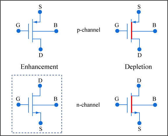
P-channel MOSFET Depletion and Enhancement Mode
The drain and source terminals are heavily doped in the p+ region, and the main substrate is n-type.
The current flows due to the flow of the positively charged carriers called holes, hence the term p-channel MOSFET.
When we apply -ve voltage to the gate terminal, electrons present under the oxide layer experience repulsion and are pushed downward into the substrate.
The depletion region is occupied by the bound +ve charges, which are associated with the donor atoms.
The -ve gate voltage attracts the positively charged holes from the p+ source and drain region into the channel.
N-channel MOSFET Depletion and Enhancement Mode
The drain and source terminals are heavily doped in the n+ region, and the main substrate is p-type.
The current flows due to the flow of negatively charged carriers called electrons, hence the term n-channel MOSFET.
When we apply +ve voltage to the gate terminal, holes present under the oxide layer experience repulsion and are pushed downward into the substrate.
The depletion region is occupied by the bound -ve charges, which are associated with the acceptor atoms.
The +ve gate voltage attracts the negatively charged electrons from the n+ source and drain region into the channel, and hence an electron-rich channel is formed.
Applications of Transistors
Transistors used in low-frequency, high-power applications, such as inverters, convert alternating current (AC) to direct current (DC).
Transistors are used in high-frequency applications to generate radio signals in oscillator circuits.
Transistors find applications in various electronic chip constructions.
It can also serve as a microscopic switch for amplifying or attenuating the electric current.
Transistors are utilized in digital logic circuits to create a short circuit. Thereby enabling the circuit to be switched on.
A FET can be used as a buffer amplifier,phase shift oscillator, voltmeter, low-noise amplifier, or analog switch.
FET is used to reduce the loading effect.
MESFET (Metal Semiconductor Field Effect Transistor) is used in high-frequency applications such as microwave circuits.
_______________________________________________________________________
See Also -
Order Electronics Projects
Want us to guide you through your project or make the project for you? Click on the button below or reach out to us via Call/WhatsApp at (+91) - 7600948607
You can -
Order Basic Electronics Projects
Order Embedded Systems Projects
Order IoT Projects
Order FPGA Projects
Order VLSI Projects
Order Image Processing Projects
Order Matlab Projects
Order TinkerCAD Projects
Order Proteus Projects
Click on the button below to fill out the project inquiry form -
Create Various Projects
Check out our Free Arduino Projects Playlist - Arduino Projects
Check out our Free Raspberry Pi Projects Playlist - Raspberry Pi Projects
Check out our Free TinkerCAD Projects Playlist - TinkerCAD Projects
Check out our Free IoT Projects Playlist - IoT Projects
Check out our Free Home Automation Projects Playlist - Home Automation Projects
Check out our Free NodeMCu Projects Playlist - NodeMCu Projects
Follow us -
Please do follow us i.e. #learnelectronicsindia to get daily updates about new blogs, videos, courses, products, offers, competitions, quizzes, and Internship Opportunities.
Using technology to increase access to youth mental health support may offer a practical way for young people to reach guidance, safe-spaces, and early help without feeling overwhelmed by traditional systems. Digital platforms, helplines, and apps could give them a chance to seek support privately, connect with trained listeners-orexplore resources that might ease their emotional load. This gentle shift toward tech-based support may encourage youth to open-up at their own pace, especially when in-person help feels too heavy to approach.
There is always a chance that these tools-quietly make support feel closer than before, creating moments where help appears just a tap away. Even a small digital interaction might bring a sense of comfort. And somewhere in that space, you…
Detailed and practical, this guide explains concrete rebar in a way that feels approachable without oversimplifying. The step by step clarity is especially useful for readers new to the subject. I recently came across a construction related explanation on https://hurenberlin.com that offered a similar level of clarity, and this article fits right in with that quality. Great شيخ روحاني resource. explanation feels practical for everyday rauhane users. I checked recommended tools on https://www.eljnoub.com
s3udy
q8yat
elso9
Strong structural training strengthens understanding of design and analysis. Well-rounded learning supports better engineering work. The guide to structural engineering courses from the college of contract management offers structured learning insight.
The current understanding of the history of atom is dominated by the Quantum Atomic Model, which replaced fixed orbits with electron clouds. Developed by scientists like Schrödinger and Heisenberg, this model uses probability to describe where an electron is likely to be found.
Career comparisons in construction regularly include salary for a bricklayer as a key factor. Bricklayers often progress into supervisory roles over time. Structured learning is offered by the College of Contract Management UK.